info@biomedres.us
+1 (502) 904-2126
One Westbrook Corporate Center, Suite 300, Westchester, IL 60154, USA
Site Map

Received: July 19, 2023; Published: August 08, 2023
*Corresponding author: Hamid Abbasi, Department of Physics, University of Mazandaran, Iran
DOI: 10.26717/BJSTR.2023.52.008201
In this research, we will seek to design and numerically evaluate a refractive index nano-sensor based on the resonant system with a metal insulating metal waveguide (MIM) that forms a wide range of wavelengths. To design the proposed sensor structure, we use two cavities and two rings with different dimensions and two plasmonic waveguides. After designing the sensor structure, we examine the resonant wavelengths and refractive index of the resonators by the finite difference method of the time domain, because this method directly obtains the Maxwell equations by proper separation in the two time and space domains and Tells us how to design the dimensions and coordinates of the sensor structure to achieve the desired result. We also draw all the diagrams of this sensor using MATLAB software. At the beginning of the simulation, we send an electromagnetic wave to the sensor structure that we have designed, through which we analyze the field distributions and the spectral response of the structural parameters. When the field distribution in a structure is the same, the energy loss is reduced. To achieve the maximum field distribution in the structure, all dimensions must be optimal. Intensification of the surface plasmon at the boundary between a metal surface and the dielectric material (sensor structure and waveguides) will increase the electric field strength and correct the sensor performance. Nanoparticle surface plasmon resonance depends on five factors: size, shape, nanoparticle composition, particle distance, and refractive index of the nanoparticle environment.
These five factors affect the wavelength and intensity of the peak. To measure sensor performance, we will calculate factors such as resolution, transmission efficiency, adjustable range of wavelengths, S sensitivity coefficient, figure of merit (FOM), Q quality factor, and quality and width factor at half the maximum (FWHM). This allows us to obtain a functional plasmonic sensor. By increasing the number of amplifiers, the FWHM of the resonant wavelength can be modulated, and reach a sensitivity of 2713 nm/RIU is realized in the near-infrared region. This sensor is suitable for use in fully integrated circuits as well as for the detection of chemical, biological and biological materials due to its high resolution accuracy, low size, high FOM value and high sensitivity coefficient.
Keywords: Optics; Plasmonics; Plasmon Surface Polaritons; Insulation Metal; Refractive Index Sensor
Abbreviations: MIM: Metal Insulating Metal Waveguide; SPP: Surface Polariton Plasmon; IMI: Insulated Metal-Insulated Structures; FOM: Figure of Merit; FWHM: Quality and Width Factor at Half The Maximum; FDTD: Finite Difference Simulation
Optical integrated circuits are one of the most important and practical tools in technology. To reduce obstacles and make more use of them, we need to shrink and compress plasmonic structures to achieve fully integrated high-efficiency optical devices. Plasmonic science has been described as the interaction of radiant electromagnetic waves to the surface of metals and their conducting electrons and has the ability to enclose electromagnetic waves at dimensions much smaller than the radiant wavelength. Plasmonics are divided into superficial plasmon plasmons [1-3] and localized superficial plasmons [4,5]. The surface polariton plasmon (SPP) is a transverse electromagnetic wave that is confined to the interface between metallic and dielectric materials and is capable of propagating up to several micrometers [6-8]. The ability of superficial polariton plasmon to overcome the limitations of classical optical diffraction has made them attractive as carriers of energy and information in circuits and optical devices. Among the various SPP structures, insulated metal-metal structures (MIM) and insulated metal-insulated structures (IMI), two common types of plasmonic structures (such as filters [9], couplers [10], sensors [11-19], etc. ...) that can be used to guide, amplify, and modify light fields at the nanoscale. Due to the support modes, high group speed, very high optical confinement and acceptable propagation length, we choose the metal insulation structure (MIM). Also, the most important plasmonic components are based on the structure of active and inactive devices.
Active environments are anisotropic and can be changed by applying an external factor, their refractive index and wavelength, ie they are suitable for switches and sensors, and inactive environments are isotropic and have only one refractive index, ie for switches and The sensors are not suitable. To build quality plasmonic sensors, parameters such as high transmission efficiency, high quality factor, high resolution, optical stability, sensitivity enhancement and adjustability in a range of wavelengths must be considered. Improving these parameters strengthens and increases the speed of information processing in optically integrated circuits. In this research, a set of plasmonic waveguides and resonators (MIM) are used to design and build our desired sensor. By analyzing this set, we seek to achieve the desired parameters in plasmonic sensors and its improvement and development. In this study, instead of changing the refractive index of all structures, we change only the refractive index of one structure and the rest of the structures have a constant refractive index. The purpose of this work is to challenge the quality of the sensor and achieve the best type of sensor performance.
Each waveguide with any kind of geometric shape is capable of transmitting waves and can limit their energy in one and two dimensions. This transition is interpreted by the wave equation. The geometry of a waveguide indicates its function, and the frequency of the transmitted wave determines the size of a waveguide. We also know that Maxwell’s equations describe the shape of electromagnetic cross waves, and the linear electricity equation describes the shape of sound waves. At longer wavelengths, wider wavelengths are guided, and at higher frequencies, narrower wavelengths will be guided. Above a frequency range, the optical properties of metals are explained by the plasma model, which is the result of Maxwell’s equations, and electrons are damped by collisions with the frequency υ = 1/τ [20]. For visible frequencies (microwave and far infrared), the spectrum of metals is very reflective and does not allow electromagnetic waves to propagate through them. At higher frequencies (near-infrared and visible from the spectrum) the field penetration and dissipation increase. Then, at ultraviolet frequencies, the metals acquire dielectric properties and allow the propagation of electromagnetic waves with different degrees of attenuation. In the free electron model at high frequencies, the dielectric function tends to zero, and for noble metals, generalizing this model to a frequency range greater than the plasma frequency creates a polar environment. As a result, real metals are expressed by the greeting model:
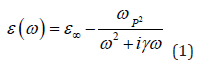
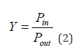
is the angular frequency, ε∞ = 1 is the dielectric constant of infinite frequency, 1.37 1016 ωp = × is the plasma frequency and γ = 3.21 × 10¹³ is the electron oscillation frequency. The Droud model provides a microscopic description of metal dynamics in the form of classical sentences. To design the desired sensor and evaluate its performance, we add rims and cavities step by step to the simulation. The Droud model provides a microscopic description of metal dynamics in the form of classical sentences. To design the desired sensor and measure its performance, we add rims and cavities to the simulation step by step. The proposed structure is shown in Figure 1, which consists of two waveguides and a ring located in the middle of the two waveguides. The ring has an inner radius of r1 = 95 nm and an outer radius of R1 = 133 nm and its distance from the two waveguides is 12 nm. The height of the two waveguides is w1 = 50 nm and the input wave goes from the left waveguide to the structure and after passing through it reaches the output waveguide. Pin and Pout are monitors that measure the input wave and the output wave, respectively, by calculating the natural component of the Poynting vector along the blurred lines. The wave transfer is calculated by the following equation:
We consider the simulation bed as silver and the environment inside the cavaties and waveguides as air. Due to the importance of the width of the resonance modes and also to achieve more accurate results, we use the experimental refractive index of silver. Also, due to the smaller width of the waveguides than the wavelength of the radiated light, there is only the fundamental TM state in the sensor structure. According to Figure 1, the TM wave begins to move with a strong magnetic field from the left and propagates in the waveguide to reach the end of the path. Wave TM in motion the closer it gets to the output, the less intense it becomes. Each resonator reflects a portion of the input wave. The scattering relationship of this fundamental state is expressed as follows [21]:
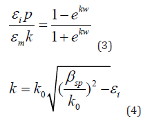
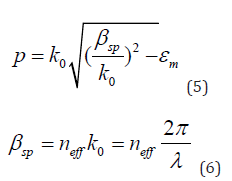
Here ω refer to the width of bus waveguide, λ shows incident light wavelength in vacuum, εi and εm give the relative dielectric and metal permittivity, βspp and neff are propagation constant and effective refractive index of SPPs, and = 2π/λ k0 means wave number. Many MIM-designed plasmonic sensors use two-dimensional simulation to test the performance of devices.
Figure 1

Figure 2

We examine the resonance behavior of the proposed sensor numerically and theoretically. For the numerical method, we use the time domain finite difference simulation (FDTD) method so that the input wave has less reflection. This method has a layer boundary condition (PML). The uniform mesh size for the x and y directions is 8 nm. We also use the transmission line model to analyze the theory of sensor structure. By changing the refractive index of the sensor, we obtain the change in wavelength in the range of 400 to 1500 nm and plot the transmission spectrum obtained from the sensor device to examine the modes obtained from the transmission. As shown in Figure 2, the sensor transmission spectra have three peaks. The peaks on the left have a Higher height and FWHM narrower, but the rate of change of the resonance wavelength in these two peaks is low, and the peak on the right has a greater change in wavelength. The first and most important factor that evaluates the performance of the sensor in question is the sensitivity S, which is calculated by Equation 7:

In this equation, is the change in resonance wavelength and is the change in refractive index In this simulation, we change the refractive index of the middle cavity with steps of 0.01 nm from n= 1.07 to n= 1.13 to start the design of the desired sensor. Using Figure 3, plot the rate of refractive index change for the change in resonant wavelength and examine it, and we conclude that according to this diagram, there is a relatively linear relationship between the two parameters of the resonance wavelength and the refractive index of the sensor. Also the TM wave resonance gradually shifts. As a result, using Equation 7, we obtain the sensitivity of different wavelengths. According to Figure 4, the maximum sensitivity for the refractive index is n = 1.13 (in mode3), which is equal to 1424 nm / RIU, and the lowest value is for the refractive index n = 1.08 (in mode1), which is equal to 330.2. Therefore, mode 3 is more sensitive than mode1 and mode2. Since sensitivity alone is not a measure of good performance for comparing different types of sensors, and light resolution is very important for sensors, we need two more to measure the capabilities of a plasmonic sensor: Q quality factor and figure of merit (FOM). Higher sensitivity reduces the FOM at the desired point. Also, increasing the length of the resonators will improve performance and reduce FOM by lengthening the light path and wasting more energy. The figure of merit (FOM) is obtained from Equation (8):
Figure 3

Using Equation 8, we plot figure of merit (FOM) diagram. According to Figure 4, the maximum value for the figure of merit (FOM) is at refractive index n = 1.13 (in mode1), which is equal to 17.259 nm / RIU. We also conclude that mode 1 has higher figure of merit (FOM) and mode 3, which had a higher sensitivity factor, has smaller figure of merit (FOM) Figure 5. The quality coefficient is also obtained from Equation 9 by dividing the wavelength by FWHM:

Figure 4

Figure 5

Figure 6

We see the quality coefficient diagram in Figure 6, the highest value of which is related to the refractive index n = 1.08 (in case 1), which is equal to 20.072 nm / RIU, and the lowest value is related to the refractive index n = 1.13 (in case 3). Which is equal to 10.416 nm / RIU. Now we add to the sensor structure a ring with inner radius r2 = 80 nm and outer radius R2 = 120 nm and a cavity with length L1 = 92 nm and height W2 = 200 nm (Figure 7). These ring and cavity that are stuck together at the bottom of the waveguide are on the right. To measure the sensor performance and calculate the sensitivity coefficient, figure of merit (FOM) and Q quality in this new structure, we only change the refractive index of the middle ring and the refractive index of the waveguides, and the cavity and the lower ring remain the same. This makes the sensor structure more challenging, and we get more accurate results. Next, we calculate the change in the refractive index of the sensor in the wavelength range of 400 to 1500 nm and obtain the resulting transmission spectrum (Figure 8). Three peaks are obtained, with the two left peaks having a higher height and a narrower FWHM, but the right peak having a lower height and a wider FWHM. Also, the right peak in this figure has a wider FWHM and higher wavelength transmission than the right peak in Figure 2, which indicates that the structure of Figure 7 will have a higher sensitivity coefficient than the structure of Figure 1. Again, we plot the refractive index changes in the selected wavelength range for the new structure and draw a graph for the relationship between the two resonant wavelength parameters and the refractive index (Figure 9).
Figure 7

Figure 8

Figure 9

According to the figure, peak 3 has better conditions than the other two peaks, and the wavelength at this peak is higher than the other two peaks. We now need to obtain the sensitivity of the different wavelengths using Equation 7. According to Figure 10, the highest sensitivity is for the refractive index n = 1.09 (in mode3) which is equal to 2673 nm / RIU and the lowest value is for the refractive index n = 1.08 (in mode1) which is equal to 199 nm / RIU. Using the sensitivity coefficient, we calculate the figure of merit (FOM) and then plot it (Figure 11). As shown in Figure 1, Peak 1 has less FOM and peaks 2 and 3 have more variations and are strongly dependent on the change in wavelength. As a result, the maximum value of figure of merit (FOM) for refractive index n = 1.09 (in mode3) is equal to 17.049 nm / RIU. The quality factor Q diagram of this sensor is obtained using Equation 9 (Figure 12) The highest value of Q quality coefficient is related to refractive index n = 1.08 (in mode2) which is equal to 18.887 nm / RIU and its minimum value for refractive index n = 1.08 (in mode3) is 7.74 nm / RIU. Now we add a rock with length L2 = 92 nm and height W3 = 200 nm to (Figure 13). The left of the structure. The distance between the two cavities is 278 nm and their distance from the waveguides is 42 nm. Naturally, the structure of the sensor faces a new challenge, so we re-evaluate the numerical factors of the sensor. Like the previous two simulations, this time we only change the refractive index of the middle ring in the range of 400 to 1500 nm to test the sensor and we keep the refractive index of waveguides and cavities and the lower ring constant. As a result, we obtain the resulting transmission spectrum (Figure 14).
Figure 10

Figure 11

Figure 12

Figure 13

Figure 14

According to the figure, peaks 1 and 2 have higher height and narrower FWHM, but peak 3 has lower height and wider FWHM. Also, the peak 3 in this figure has a wider FWHM and higher wavelength transmission than the peak 3 in Figures 2 & 8. This means that this structure has a higher sensitivity coefficient than the previous structure and the designed sensor will also perform better. Our goal in adding resonator step by step was to gauge their position so that we could select more appropriate dimensions for them. We now examine the graph of the rate of change of the refractive index in the selected wavelength range for the new structure to obtain a graph of the relationship between the resonant wavelength and the refractive index (Figure 15). According to the figure, peak 3 has more wavelengths change than the other two peaks as well as the peaks of the previous two structures and as with the result in Figure 14, we again conclude that peak 3 has a higher sensitivity. The first criterion for measuring the performance of a sensor is its sensitivity. Therefore, we obtain the sensitivity of different wavelengths using Equation 7. According to Figure 16, the highest sensitivity is for the refractive index n = 1.09 (in mode3) which is equal to 2713 nm / RIU and the lowest value is for the refractive index n = 1.08 (in mode1) which is equal to 199.9 nm. We now calculate the FOM eligibility figure and plot it (Figure 17). The value of figure of merit (FOM) in refractive index n = 1.09, which has the highest sensitivity coefficient, reaches 18.669. Like the sensitivity coefficient, the figure of merit (FOM) has also increased compared to the previous structure.
Figure 15

Figure 16

Figure 17

The last criterion for measuring this sensor is the quality factor Q, the diagram of which is obtained using Equation 9 (Figure 18). The value of quality coefficient Q in the refractive index n = 1.09, which has the highest sensitivity coefficient, reaches 8. 458.As shown in Table 1, the proposed method offers better results compared to some similar articles. According to this table, the maximum value of S sensitivity coefficient among these papers belongs to the structure studied in this paper, which is equal to 2713 nm. Figure 19 shows the plasmonic sensor field distribution when it reaches its maximum sensitivity of 2713 nm / RIU. The field distribution in the rims is much more than two cavities. Also, the middle ring has a larger field distribution than the right ring, which is because during the simulation we only changed the refractive index of the middle ring. For this reason, the middle ring makes the most changes and sees the largest field distribution and creates a transmission slope.
Figure 18

Figure 19

Table 1: Comparison between proposed sensor specifications and similar articles.

Plasmonic sensor is a broad topic and we have highlighted the latest developments in the design of refractive index sensors based on metal-insulated plasmonic waveguides. The structure of the sensor is analyzed numerically and theoretically. Theoretical and numerical results are obtained using the transmission line model and the time difference finite difference method, respectively. Theoretical results are consistent with numerical results. In several plasmonic resonator designs discussed, we have achieved excellent sensitivities of 2713 nm / RIU and 2673 nm / RIU. This proposed device can be used in plasmonic sensing systems in the near-infrared region and improve the performance of sensors that will be designed in the future.
This research received no external funding.
The authors declare no conflict of interest.
All materials and data of this article are at the disposal of the authors.